

Semiconductor
Suitable for the following applications:
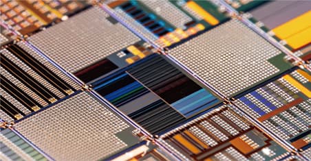
As the number of manufacturing processes increases, even tiny errors at each step accumulate, potentially leading to near-zero wafer yield. Therefore, to ensure the quality of the final product, semiconductor manufacturers must implement rigorous quality control for each process. Inspection and process control have become core elements of successful modern semiconductor manufacturing.
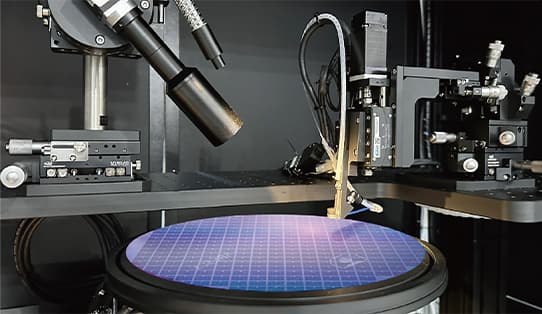

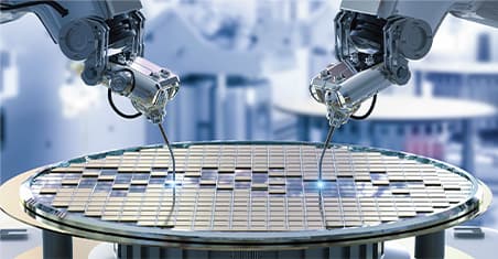
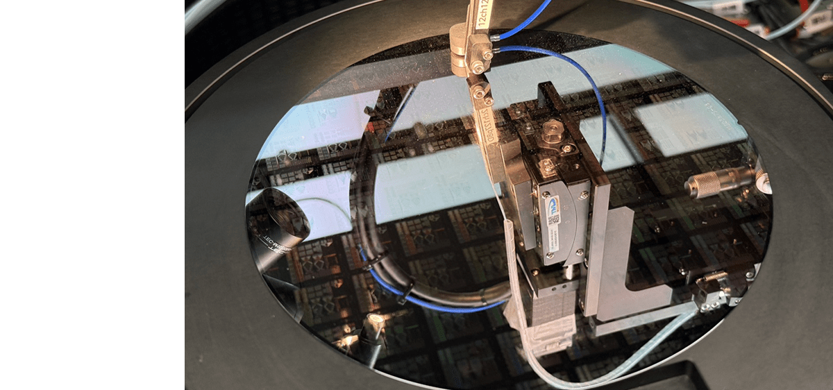
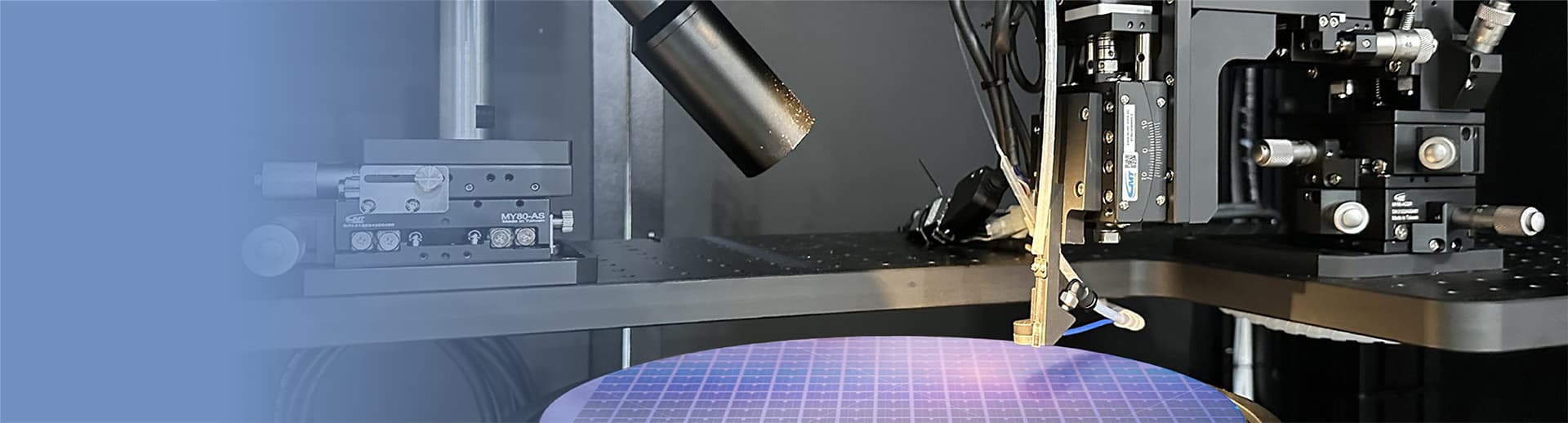
In semiconductor manufacturing, even the slightest deformation of a wafer can profoundly impact the performance and yield of the final product. For example, a wafer may develop scratches or cracks due to bending or the contact points of the chuck supporting it; these minute defects directly affect the accuracy and reliability of subsequent nanoscale processes. During AOI (Automated Optical Inspection), inspection instruments such as optical lenses need to perform high-precision measurements at the nanoscale. To accurately inspect wafer/wafer surface details, advanced precision positioning and control technology is essential to move the wafer/wafer or inspection lenses, ensuring stable and accurate alignment with the area under test.
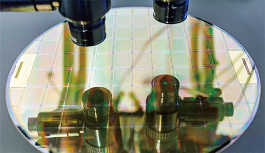
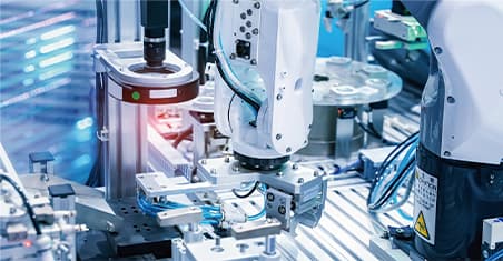
High-precision positioning technology plays a crucial role in advanced packaging and semiconductor manufacturing processes, especially in chip packaging and testing. Driven by the explosive growth in AI demand, advanced chips must simultaneously achieve high speed, energy efficiency, and cost control, making advanced packaging a global mainstream solution. The shrinking size and increasing functional complexity necessitate nanometer-level positioning accuracy in the manufacturing process to ensure that the circuitry within each chip is accurately stacked, preventing losses caused by even the slightest misalignment and thus improving production efficiency.

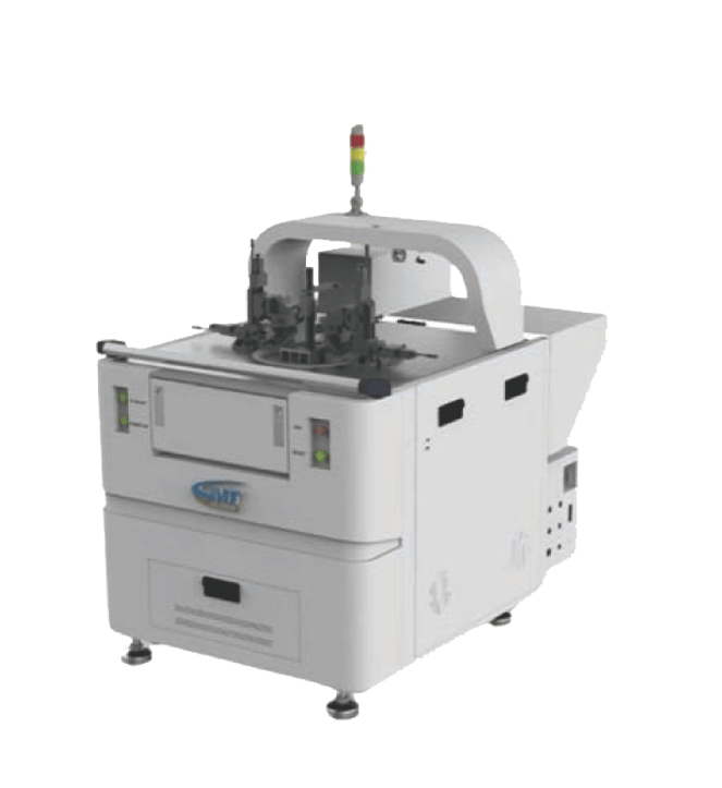
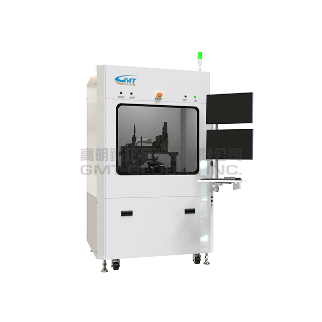
Advanced packaging technology plays a crucial role in the semiconductor industry. As wafer sizes shrink, the flatness of the bare dies and the alignment accuracy of the wafers during stacking become extremely demanding, requiring nanometer-level precision. Even slight deviations in accuracy can have significant consequences, impacting overall performance and yield. Furthermore, neglecting known-good die testing before stacking renders the advanced packaging process ineffective. Therefore, from silicon wafers to chips, rigorous optical/electrical testing, and visual inspections are essential to ensure quality, performance, and reliability, thereby improving yield and reducing costs. GMT GLOBAL provides nanometer-level high-precision positioning control technologies and manual/motorized stage products for optical testing, electrical testing, visual inspection, and advanced packaging in the semiconductor industry, offering optimal solutions for its customers.