
GMT focused optical path detection, possessing dual advantages
GMT focused optical path detection, possessing dual advantages
The explosive growth in demand for artificial intelligence (AI) computing is putting increasing pressure on data center transmission, making co-packaged optics (CPO) a key solution to overcome these bottlenecks. Analysts predict that Nvidia's Rubin architecture will see a major rollout of CPO by 2026, generating billions of dollars in revenue and rapidly driving demand across the silicon photonics components, packaging, testing, and equipment supply chain.
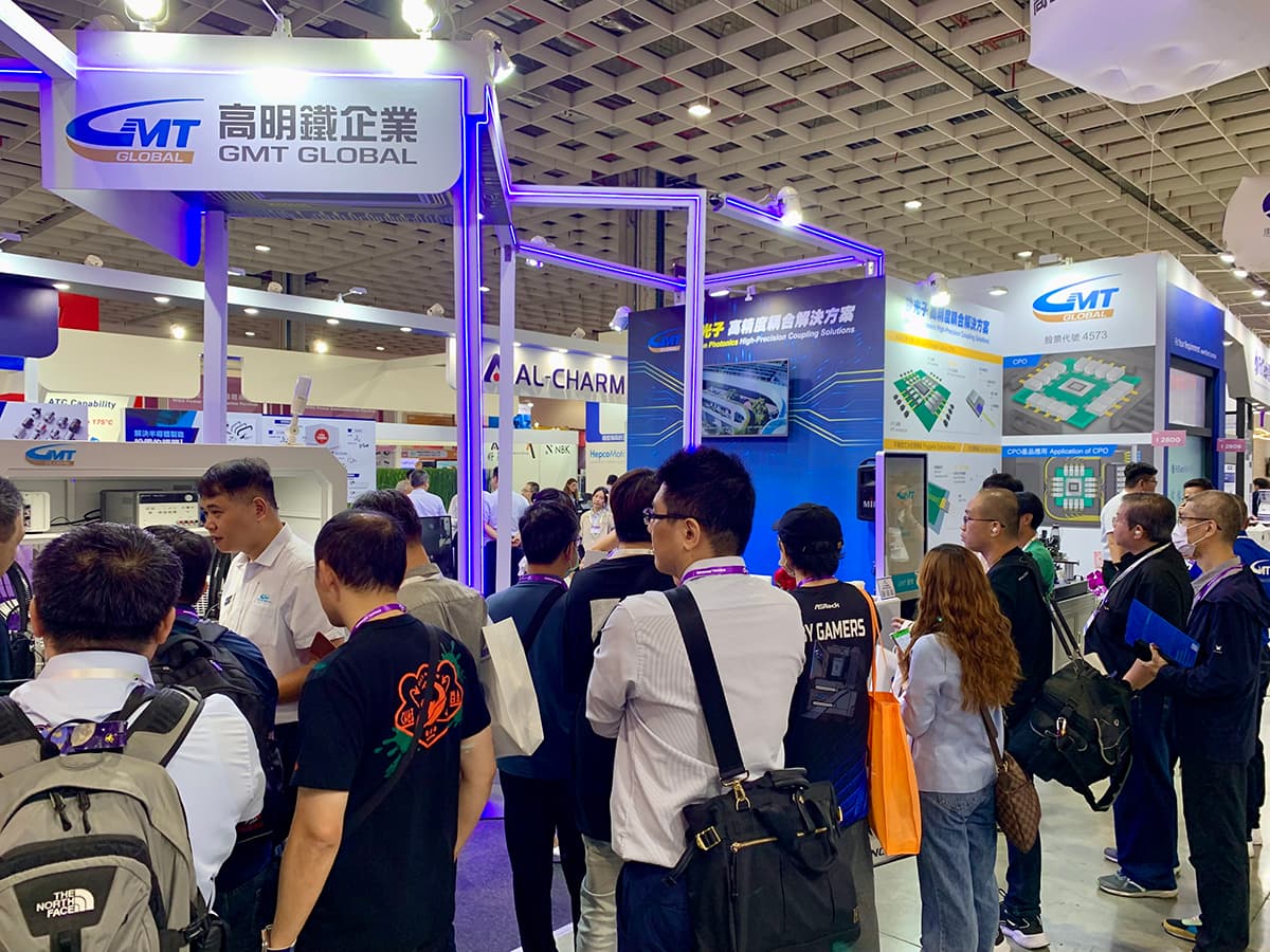
GMT unveiled its "Silicon Photonics High-Precision Coupling Solution" at SEMICON Taiwan 2025, engineering the "light finding, alignment, and light locking" process to address the pain points of CPO mass production. One of the biggest challenges in silicon photonics packaging is yield; any minute error can lead to a decrease in transmission efficiency. Therefore, high-precision and high-stability optical coupling equipment has become a core critical factor.
The "Silicon Photonics Active Alignment and Wafer-Level Optical Coupling Test Platform" showcased at the event combines a six-axis high-precision platform, AI algorithms, and 6D laser measurement to transform optical alignment, which previously relied on manual experience, into a standardized process. Through optical scales and error compensation, the accuracy can be improved from 0.5 micrometers to the 50 nanometer level, significantly reducing the impact of alignment errors on yield.
The platform supports stacked and Stewart parallel architectures, suitable for CPO optical engines, AI server optical modules, and silicon photonics wafer testing, with bandwidth ranging from 800G to 1.6T. Plans are in place to extend to 3.2T and 6.4T optical transceiver modules, fully meeting the upgrade needs of next-generation data centers and telecom backbones. In the future, GMT will also attempt to integrate the advantages of dynamic and static accuracy to create a dual-mode parallel solution, balancing R&D verification and large-scale mass production.
In terms of competition, while foreign manufacturers possess deep technological expertise and mature products, their designs tend to be standardized and uniform. Although their implementation processes are complete, they are less capable of customization and responsiveness. In contrast, GMT 's advantage lies in its localization. It can be close to the Taiwanese supply chain, quickly adjust designs and algorithms according to customer needs, shorten development cycles, and improve yield rates, which is more in line with the rapid iteration pace of the Asian semiconductor industry chain.
With NVIDIA and Taiwanese companies jointly advancing CPO technology, the market is rapidly taking shape. NVIDIA's networking division points out that the Rubin series uses a micro-ring modulator (MRM), improving power efficiency by 3.5 times and network flexibility by 10 times. Taiwan's leading wafer foundry emphasizes that silicon photonics can solve the "memory wall" effect and has established a complete PDK, covering waveguides, splitters, and multiplexers, driving the commercialization of photonic integrated circuits (PIC). Analysts predict that by 2030, CPO will account for over 50% of high-speed transmission solutions, simultaneously benefiting the silicon photonics supply chain.
GMT is also actively promoting the localization of silicon photonics workstations, joining the SEMI Silicon Photonics Industry Alliance SIG2, and aligning with the National Development Council's "Ten New AI Constructions" policy to plan and build a shared measurement and coupling platform, and promote the standardization of fixtures and processes. Through local supply chain collaboration, GMT hopes to form a complete chain of "design-process-testing-assembly," becoming an important part of Taiwan's silicon photonics ecosystem.
Source: TechNewshttps://technews.tw/2025/09/11/ GMT -cpo/