
GMT silicon photonics high-precision coupling facilitates the mass production of CPO.
GMT silicon photonics high-precision coupling facilitates the mass production of CPO.
Generative AI is driving the rapid upgrade of data centers, with silicon photonics becoming a key technology for low power consumption and high bandwidth. It is believed to be an essential technology for high-speed transmission in NVIDIA's next-generation AI servers, rapidly propelling the rise of the CPO process wave. GMT (4573.TWO) unveiled its "Silicon Photonics High-Precision Coupling Solution" at SEMICON Taiwan 2025 (Nangang Hall 1, 1F: I2800). By "active alignment + wafer-level optical coupling testing," the solution engineered the processes of finding, aligning, and locking light, accelerating the mass production of CPO. Analysts predict that GMT is likely to become a highlight among silicon photonics concept stocks.
GMT holds a leading position in the fields of silicon photonics and co-packaged optics (CPO). Integrating a six-axis platform, AI image servo, and 6D laser metrology, GMT covers everything from light finding to alignment. It is applicable to CPO optical engines, AI server optical modules, silicon photonics wafer testing and packaging, supporting speeds from 800G to 1.6T and expanding to 3.2T/6.4T optical transceiver modules and CPO application requirements. GMT provides a complete solution of "active alignment + wafer-level optical coupling testing," meeting the upgrade needs of data centers and telecom backbones, and becoming a powerful tool for mass production of CPO in the AI era.
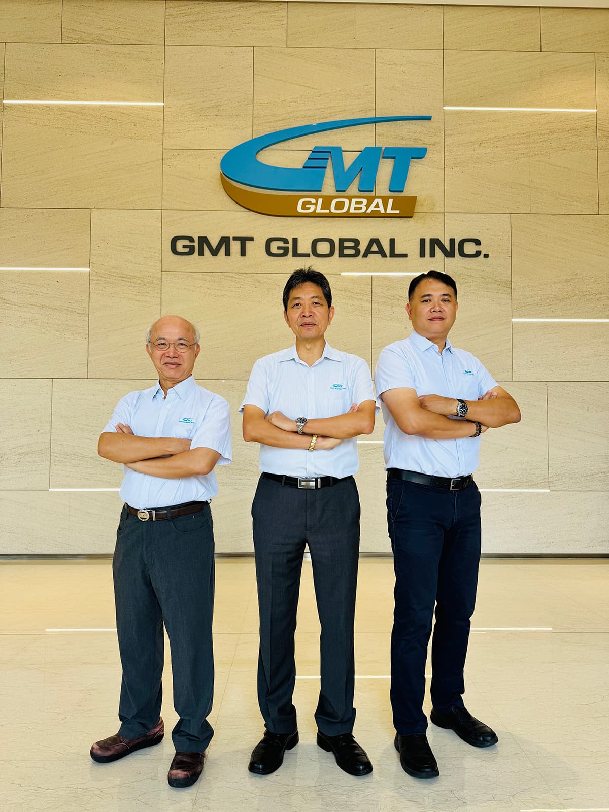
Lin Chin-hui, deputy director of GMT Precision Control Business Unit, pointed out that GMT is focusing on key silicon photonics technology - optical coupling. The new generation "Silicon Photonics Active Alignment and Wafer-Level Optical Coupling Test Platform" will be showcased at this year's Semiconductor Show. With its four-in-one engineering capabilities of "mechanism + control + algorithm + measurement", it standardizes and modularizes the alignment and optical coupling process of silicon photonics, fully meeting the needs of data centers, high-speed switches, and the mass production requirements of common packaged optics (CPO).
Lin Chin-hui stated that the focus will be on the technological independence of domestically produced testing equipment and key workstations, assisting Taiwan's silicon photonics ecosystem in forming a complete ecosystem from "design, process, testing to assembly". The AI era requires not only faster "computing power" but also more stable "optical paths". GMT 's mission is to transform "finding light, aligning, and locking light" into a replicable, verifiable, and mass-producible process.
In June 2025, the National Development Council (NDC) included silicon photonics in its "Top Ten New AI Development Plans," planning to invest in the supply chain through the NDC Fund, establish silicon photonics research centers, introduce shared testing equipment, actively purchase silicon photonics testing equipment for R&D sharing within the industry ecosystem, and encourage the development of domestically produced testing equipment. GMT joined the SEMI Silicon Photonics Industry Alliance SIG2, becoming part of Taiwan's silicon photonics ecosystem. In addition to sharing knowledge, resources, and expertise, the alliance aims to lead the future era of rapid technological advancement together with its members.
Regarding GMT "Silicon Photonics Active Alignment and Wafer-Level Optical Coupling Test Platform," the biggest highlight is the integration of technologies such as mechanisms, control, algorithms, and measurement, which transforms uncertainty into an engineering process. Lin Jinhui further explains this below:
I. Six-axis high-precision platform (stacked + Stewart parallel type):
- Stacked type: linear single-axis repeatability can reach ±0.05μm; rotary axis repeatability is ±5μrad.
- Stewart parallel system: excellent dynamic response, flexible multi-axis synchronization; linear repeatability ±0.15μm, rotation ±3μrad. Two platforms meet different timeframes from R&D to mass production and can be quickly transitioned using a unified control language.
II. Pose Measurement and Error Compensation:
- Stacked tables are used for error compensation via single-axis table creation; and the Stewart platform returns to the kinematic equations, mapping minute deviations in actuator and fulcrum assembly into pose errors and correcting them via closed-loop. Additionally, fixture rotation fulcrum offset correction ensures the fulcrum does not drift during end-face angle adjustments, substantially reducing coupling loss.
III. AI Active Alignment Algorithm (Image Servo × Light Feedback):
- Visual Servoing: Captures edge lines and corner points from both top and side views, calculates slope, angle, and center point, and quickly completes end face "alignment".
- Light gradient convergence: After reaching the First Light, the gradient direction is estimated by real-time light feedback to accelerate convergence to the global maximum; if the threshold is not reached, the angle is finely adjusted by a similar optimization mechanism.
- Area scanning + peak estimation: Provides scanning trajectories such as spiral, sine, sawtooth, triangular and square waves; after scanning, the peak position is estimated by fitting a Gaussian distribution, and multiple parameters can be connected in series to form a "scanning sequence" to improve the success rate of one-time positioning.
IV. Integration of Domestic Machine Drive and Control System for 6D High-Precision Laser Measurement:
- 6D laser measurement system: linear accuracy error < 0.5 ppm, angle detection error < ± (1.0arcsec + 0.1arcsec/m), supporting equipment optical coupling accuracy of less than 50 nm.
- EtherCAT multi-axis synchronization, HMI user-friendly parameter tuning, and TCP/IP Socket connectivity make it easy to integrate into MES and test station recipes, forming a traceable and replicable mass production process.
- Key components are manufactured in-house and processed and inspected at the nanometer level, with overall repeatability better than ±50nm, ensuring cross-machine consistency.
From Wafer to Module: Optical Coupling and Testing Capabilities of Silicon Photonics Total Solution
- Wafer Level (WLP): Supports waveguide characteristic detection and multi-channel automatic alignment measurement, improving site throughput and cross-machine consistency.
- Module-level and CPO: It can serve as a standard workstation (AA Cell) for CPO alignment and assembly, supporting optical engines of 800G and above, and is prepared to be introduced into 1.6T mass production, with plans to extend to 3.2T and 6.4T; at the same time, it supports the CPO nodes required for 51.2T switches.
- Extended applications: biomedical sensing, autonomous vehicle LiDAR and other multi-faceted opto-electro-mechanical integrated testing, forming an expandable family of solutions.
The National Development Council's "Ten New AI Development Initiatives" plan allocates resources to silicon photonics and shared testing, supported by policy and ecosystem collaboration. Lin Chin-hui emphasized that GMT will further collaborate with research institutions and industry partners to build a "Silicon Photonics Shared Measurement/Coupled Laboratory," promoting the standardization of domestically produced testing equipment. Shared demonstration line: Based on the GMT platform, it will facilitate measurement verification and parameter management for industry, academia, and research. Standardized fixtures and processes: From multi-channel fiber array clamps to end-face angle calibration, consistent delivery and maintenance. Local supply chain: Collaborating with upstream actuator, sensing, and optoelectronic module manufacturers to implement a localized solution of "local procurement and upgradeability."
Source: Economic Dailyhttps://money.udn.com/money/story/5735/8985170